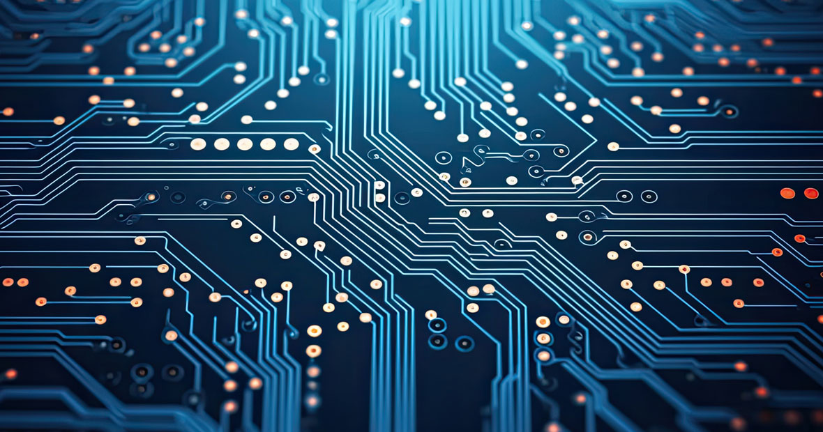
Peeling back the layers to reveal the intricate world of HDI PCB manufacturing, one finds a fascinating blend of art and science. This process, a cornerstone of modern electronics, employs cutting-edge technology and meticulous precision to produce compact yet highly functional circuit boards. Starting from the basic assembly of essential components, every stage of HDI PCB production demands a keen attention to detail. The adoption of new materials and innovative design strategies contributes significantly to this precision, while quality control ensures the reliability of the final product. Yet, despite the advancements in technology, achieving perfection in HDI PCB layering is still fraught with challenges, be they technical hurdles or constraints imposed by materials. Delving deeper into this realm, one uncovers the solutions to these obstacles, underscoring the resilience and ingenuity inherent in the field of electronic design and assembly.
Unraveling the Complexity of HDI PCB Manufacturing
Delving into the intricacies of High-Density Interconnect (HDI) Printed Circuit Board (PCB) production uncovers a sophisticated process, steeped in precision and meticulous attention to detail. The modern world of electronics depends heavily on this technology, given its eminent role in enhancing the efficiency and performance of contemporary devices.
Essential Components Involved in HDI PCB Production
Manufacturing high density PCBs poses significant technical challenges due to their increased density. The primary components – copper and rigid layers – form the backbone of these boards. PCBA manufacturers employ advanced processes, leveraging the latest technology to overcome these challenges. The fine intricacies of placing multiple components onto a small chip require a high degree of precision, a testament to the skills of the manufacturer.
Process Stages of HDI PCB Manufacturing
From concept to production, each stage in the HDI PCB manufacturing process adds a new layer of complexity. Initial data preparation sets the stage, followed by a series of steps including multilayer assembly and copper plating. The final test phase ensures the quality and functionality of the finished product, a critical step in an industry where reliability is paramount.
Importance of Quality Control in HDI PCB Manufacturing
Quality control plays a pivotal role in HDI PCB production. Despite the high cost, manufacturers cannot compromise on this aspect due to the long-term implications on the device’s performance. Every PCB manufacturer, including icape-group.com, invests heavily in quality assurance, affirming the importance of this aspect in the entire process.
Looking ahead, the future of HDI PCB manufacturing will continue to evolve with ongoing technological innovation, creating new challenges and opportunities for manufacturers across the globe.
Interplay of Art and Science in HDI PCB Precision Layering
In an environment where perfection is mandatory, the importance of precision in the layering of HDI PCB manufacturing is paramount. By intertwining art and science, perfect precision in HDI PCB layering is achieved. The scientific techniques employed serve the need for precision. For instance, the use of vias in the PCB layers enhances electrical connectivity. The surface of the PCB, therefore, requires a careful and meticulous process of plating. Because the process is detail-oriented, it mirrors the meticulous nature of art.
Art plays a significant role in the design and production of HDI PCB layers of high precision. The application of artistry ensures the production of the best quality PCBs. Each layer is like a canvas, where the artist paints with precision to create a masterpiece. In the same vein, the PCB layers must be meticulously and artistically designed to ensure optimal functionality. The challenges faced in the precise layering of HDI PCBs are overcome by the harmonious marriage of art and science. The solutions therein lie in the precise application of artistic creativity and scientific techniques.
-
Artistry in design: The creative process involved in designing PCB layers helps ensure precision and functionality.
-
Scientific techniques: The use of vias and other scientific techniques enhances the precision of the HDI PCB layers.
-
Challenges and Solutions: The challenges faced in HDI PCB layering are overcome by the harmonious blend of art and science in fabrication.
Role of Technological Innovation in Enhancing HDI PCB Manufacturing Precision
Technological innovation plays a pivotal role in enhancing the precision of HDI PCB manufacturing. It promotes high levels of accuracy and reliability in the production process. The positive impact of such technological advancements is clearly visible in the industry, allowing manufacturers to overcome various challenges and consistently deliver high-quality products.
With the introduction of new materials and processes, the manufacturing of HDI PCBs has seen a significant revolution. These new technologies are critical in maintaining competitiveness in an ever-evolving industry. The best example of this is the use of advanced testing methods to ensure the accuracy and functionality of the finished product. These tests provide a quality assurance that is integral to the success of any PCBA.
The manufacturing of these multilayer PCBs requires extreme precision, and technological innovation has been pivotal in achieving this. Each layer must be meticulously crafted and tested to ensure its functionality and reliability. This level of detail is only possible through the use of advanced manufacturing processes and materials, made possible by ongoing technological innovation.
Industry leaders have adopted these new technologies and processes to stay competitive, demonstrating the importance of technological innovation in this field. For instance, the use of high-tech machinery and processes, such as automated assembly and testing systems, has significantly improved the precision of HDI PCB manufacturing.
Challenges in Achieving Precision in HDI PCB Layering
Beginning with a focus on precision, mastering the art of HDI PCB layering serves as an essential determinant for optimal performance. The journey to balance miniaturization and density presents challenges that demand technical prowess.
Technical Hurdles in HDI PCB Layering
Central to HDI PCB layering, the issue of maintaining quality whilst contending with the miniaturization and density of components stands as a significant challenge. The rigid nature of vias, coupled with the ever-increasing demand for smaller, more complex boards, escalates the difficulty of ensuring precision. Notably, time and cost factors add to the complexity, necessitating efficient, cost-effective solutions.
Material Constraints Impacting Precision
Human error and material limitations further complicate the layering process. The intricacies involved in handling materials and the potential for error in execution highlight the need for meticulous attention to detail. Key to overcoming these challenges involves identifying and implementing advanced techniques and technologies.
Solutions to Overcome Precision Challenges in HDI PCB Layering
Looking towards the future, continuous learning and technological advancements promise potential solutions to the complexities of HDI PCB layering. The flex to rigid-flex boards, for instance, indicates a strategy to address these challenges. By prioritizing growth and adaptation, the industry may navigate these hurdles and maintain a commitment to precision.